- 您现在的位置:买卖IC网 > Sheet目录337 > LE25U20AMB-AH (ON Semiconductor)IC MEM 2MBIT SERIAL FLASH 8SOP
�� �
�
�LE25U20AMB�
�Device� Operation�
�The� LE25U20AMB� features� electrical� on-chip� erase� functions� using� a� single� 2.5V� power� supply,� that� have� been� added�
�to� the� EPROM� functions� of� the� industry� standard� that� support� serial� interfaces.� Interfacing� and� control� are� facilitated� by�
�incorporating� the� command� registers� inside� the� chip.� The� read,� erase,� program� and� other� required� functions� of� the�
�device� are� executed� through� the� command� registers.� The� command� addresses� and� data� input� in� accordance� with� "Table�
�2� Command� Settings"� are� latched� inside� the� device� in� order� to� execute� the� required� operations.� "Figure� 3� Serial� Input�
�Timing"� shows� the� timing� waveforms� of� the� serial� data� input.� First,� at� the� falling� CS� edge� the� device� is� selected,� and�
�serial� input� is� enabled� for� the� commands,� addresses,� etc.� These� inputs� are� introduced� internally� in� sequence� starting� with�
�bit� 7� in� synchronization� with� the� rising� SCK� edge.� At� this� time,� output� pin� SO� is� in� the� high-impedance� state.� The�
�output� pin� is� placed� in� the� low-impedance� state� when� the� data� is� output� in� sequence� starting� with� bit� 7� synchronized� to�
�the� falling� clock� edge� during� read,� status� register� read� and� silicon� ID.� Refer� to� "Figure� 4� Serial� Output� Timing"� for� the�
�serial� output� timing.�
�The� LE25U20AMB� supports� both� serial� interface� SPI� mode� 0� and� SPI� mode� 3.� At� the� falling� CS� edge,� SPI� mode� 0� is�
�automatically� selected� if� the� logic� level� of� SCK� is� low,� and� SPI� mode� 3� is� automatically� selected� if� the� logic� level� of�
�SCK� is� high.�
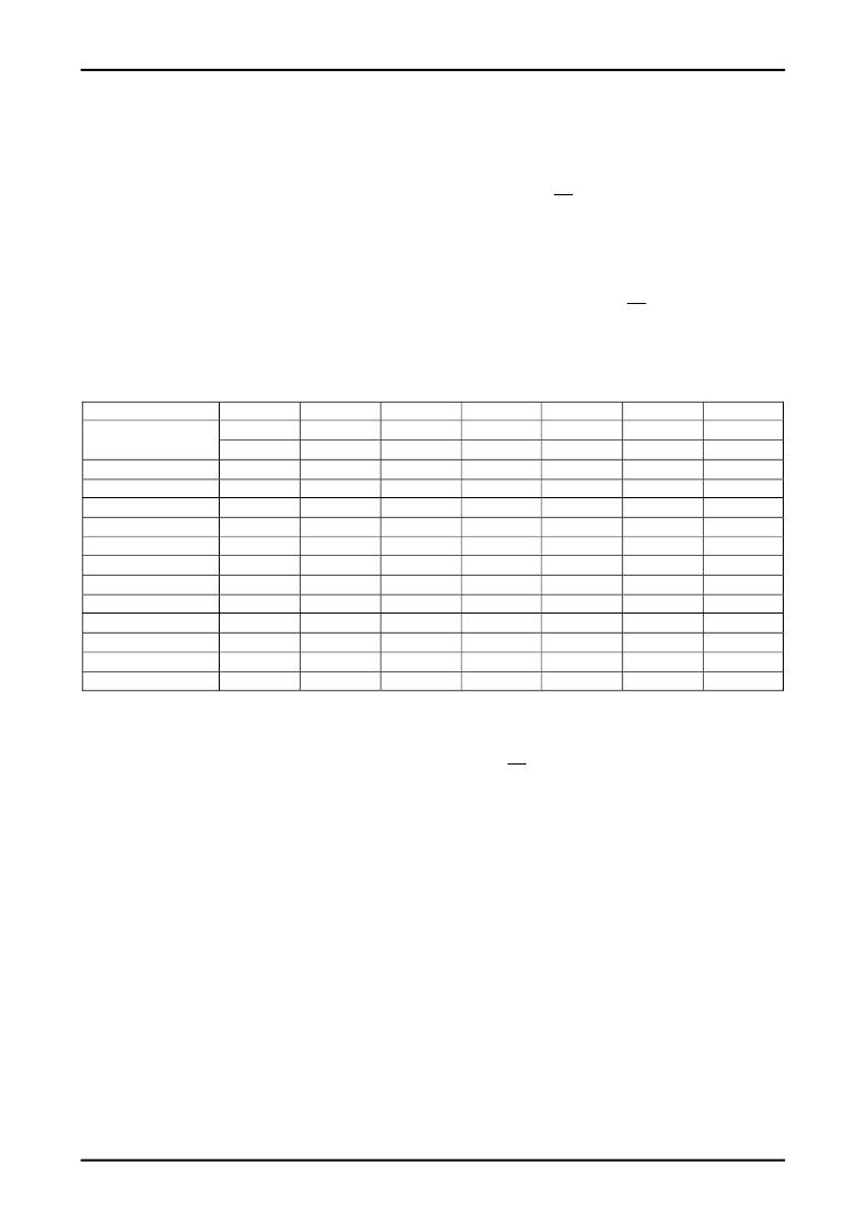
�Table� 2� Command� Settings�
�Command�
�1st� bus� cycle�
�2nd� bus� cycle�
�3rd� bus� cycle�
�4th� bus� cycle�
�5th� bus� cycle�
�6th� bus� cycle�
�Nth� bus� cycle�
�Read�
�03h�
�A23-A16�
�A15-A8�
�A7-A0�
�0Bh�
�A23-A16�
�A15-A8�
�A7-A0�
�X�
�Small� sector� erase�
�Sector� erase�
�D7h/20h�
�D8h�
�A23-A16�
�A23-A16�
�A15-A8�
�A15-A8�
�A7-A0�
�A7-A0�
�Chip� erase�
�C7h�
�Page� program�
�02h�
�A23-A16�
�A15-A8�
�A7-A0�
�PD� *�
�PD� *�
�PD� *�
�Write� enable�
�Write� disable�
�Power� down�
�Status� register� read�
�06h�
�04h�
�B9h�
�05h�
�Status� register� write�
�Read� silicon� ID� 1�
�01h�
�9Fh�
�DATA�
�Read� silicon� ID� 2�
�ABh�
�X�
�X�
�X�
�Exit� power� down� mode�
�ABh�
�Explanatory� notes� for� Table� 2�
�"X"� signifies� "don't� care"� (that� is� to� say,� any� value� may� be� input).�
�The� "h"� following� each� code� indicates� that� the� number� given� is� in� hexadecimal� notation.�
�Addresses� A23� to� A18� for� all� commands� are� "Don't� care".�
�In� order� for� commands� other� than� the� read� command� to� be� recognized,� CS� must� rise� after� all� the� bus� cycle� input.�
�*:� "PD"� stands� for� page� program� data.�
�No.A2097-4/21�
�发布紧急采购,3分钟左右您将得到回复。
相关PDF资料
LFDAS12XSIT
HARDWARE MC9S12XS 112-PIN
LFXP10E-L-EV
BOARD EVAL LATTICEXP10E STD
LH28F008SCHT-TE
IC FLASH 8MBIT 85NS 40TSOP
LH28F160S3HNS-TV
IC FLASH 16MBIT 100NS 56SSOP
LH28F160S5HNS-S1
IC FLASH 16MBIT 70NS 56SSOP
LH28F320S3HNS-ZM
IC FLASH 32MBIT 110NS 56SSOP
LH28F320SKTD-ZR
IC FLASH 32MBIT 70NS 48TSOP
LHF00L28
IC FLASH 16MBIT 70NS 48TSOP
相关代理商/技术参数
LE25U20AMBM02-AH
功能描述:闪存 RoHS:否 制造商:ON Semiconductor 数据总线宽度:1 bit 存储类型:Flash 存储容量:2 MB 结构:256 K x 8 定时类型: 接口类型:SPI 访问时间: 电源电压-最大:3.6 V 电源电压-最小:2.3 V 最大工作电流:15 mA 工作温度:- 40 C to + 85 C 安装风格:SMD/SMT 封装 / 箱体: 封装:Reel
LE25U40CFQ-AH
制造商:ON Semiconductor 功能描述:REEL / S-FLASH MEMORY(4M)
LE25U40CMC
制造商:SANYO 制造商全称:Sanyo Semicon Device 功能描述:4M-bit (512K??8) Serial Flash Memory
LE25U40CMC-AH
功能描述:闪存 S-FLASH MEMORY(4M)
RoHS:否 制造商:ON Semiconductor 数据总线宽度:1 bit 存储类型:Flash 存储容量:2 MB 结构:256 K x 8 定时类型: 接口类型:SPI 访问时间: 电源电压-最大:3.6 V 电源电压-最小:2.3 V 最大工作电流:15 mA 工作温度:- 40 C to + 85 C 安装风格:SMD/SMT 封装 / 箱体: 封装:Reel
LE25U40CMCQ00-AH
制造商:ON Semiconductor 功能描述:Flash S-FLASH MEMORY(4M)
LE25U40CQE
制造商:SANYO 制造商全称:Sanyo Semicon Device 功能描述:4M-bit (512K??′8) Serial Flash Memory
LE25U40CQE-AH
功能描述:电可擦除可编程只读存储器 RoHS:否 制造商:Atmel 存储容量:2 Kbit 组织:256 B x 8 数据保留:100 yr 最大时钟频率:1000 KHz 最大工作电流:6 uA 工作电源电压:1.7 V to 5.5 V 最大工作温度:+ 85 C 安装风格:SMD/SMT 封装 / 箱体:SOIC-8
LE25U40CQES00-AH
制造商:ON Semiconductor 功能描述:S-FLASH MEMORY(4M)